
Connecting Microns to China's Core Future: ZZT Supports the Development of Domestic Precision Testing Technology

In 2026, as AI chips, 5G communication, and high-performance computing rapidly advance, test probes, as key precision components in semiconductor testing, are gaining increasing attention from industry customers. From smartphones to AI acceleration cards, each chip undergoes rigorous testing with a test probe before mass production. As advanced technologies such as Chiplet and 3D packaging become more widespread, the testing probe industry is facing dual opportunities for technological upgrades and market demand. Gold-link, a professional manufacturer in China specializing in precision connectivity and testing, has accumulated years of technological expertise to develop and scale up test probes, making it a trusted partner in this specialized field.

Test probes are crucial consumables for determining semiconductor yield and testing efficiency. According to research by the international consulting firm Yole and CICC, the global wafer testing probe market is expected to continue growing steadily in the coming years. The increased demand for AI servers and high-performance computing places higher demands on probe accuracy, reliability, and durability. As chip manufacturing processes continue to advance and chip packaging complexity increases, probe design is trending towards finer spacing, higher frequencies, and greater durability. This means that probe companies with micro-nano manufacturing capabilities will have more development opportunities, and TopLink is a proactive player in this trend.

Looking ahead to the next three to five years, the development path for the testing probe industry is becoming increasingly clear. The process of domestic replacement is accelerating, with the high-end test probe market long dominated by overseas brands. In recent years, the overall competitiveness of domestic probes in terms of performance, delivery time, and cost has continued to improve. Meanwhile, the demand for high-frequency and high-speed probes is becoming increasingly prominent, with the development of 5G and future 6G communication, as well as the widespread adoption of high-speed interface standards like PCIe 6.0, placing higher demands on material selection and structural design. Furthermore, the trend towards smaller equipment is driving the development of ultra-fine pitch probes, with a gradual release of demand for 0.1-millimeter diameter microphones, wearable devices, and medical electronics, making it an important direction for probe technology innovation.

In this track brimming with opportunities and challenges, we have gradually developed our technical characteristics in the field of test probes through ongoing R&D investments and manufacturing capabilities. Facing the trend towards industry miniaturization, we have been able to mass-produce high-precision probes, providing reliable solutions for semiconductor wafer testing and microelectronic product inspection. At the same time, TopLink has extensive experience in Pogo Pin connectors and high-frequency probes. For applications such as AI servers and 5G communication modules, it ensures stable contact impedance and signal integrity through precise structural design and material optimization.

In 2026, as the semiconductor supply chain continues to evolve, the testing of test probes is moving from behind the scenes into the视野用户的of more industry users. For customers with precision testing needs, we are not only a supplier with probe R&D and manufacturing capabilities, but also a technological partner that provides stable products and professional services in fine connections and precise testing.
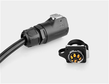
We will continue to contribute to the development of domestic precision testing technology with solid technology and reliable quality.