
Pogo Pin Contact Pad
High-reliability pogo pin contact pads featuring hard gold plating and precision manufacturing. Ideal for wearable-device charging interfaces, medical diagnostic equipment, industrial test fixtures, and board-to-board interconnects-supporting projects from prototyping through mass production.
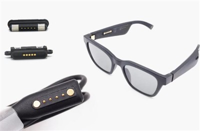
Why Pogo Pin Contact Pad Design Determines System Reliability
Most engineers focus on the pogo pin itself while treating the mating contact pad as a secondary consideration. In reality, this is often where failures occur.
Over the past 15 years, we have repeatedly observed the same failure modes across numerous projects:
Contact pads that are too small to accommodate mechanical misalignment or enclosure tolerances.
Low-quality surface finishes selected to reduce costs in products expected to withstand 50,000 mating cycles.
Direct copper-plated pad designs used for high-current applications without considering temperature rise and thermal effects.
None of these issues are particularly complex. The challenge is making the right design decisions before the first prototype is built, rather than trying to correct problems later. This is where many projects incur unnecessary delays and costs.
This page summarizes the lessons we have learned from these projects, covering contact pad dimensions, plating selection, current-carrying capability, and layout guidelines.

What Makes a Reliable Pogo Pin Contact Pad?
Reliability depends on three interacting factors: mechanical consistency, surface chemistry, and thermal margin. Optimizing only one while neglecting the others can result in a design that passes testing but fails in real-world use.
Mechanical Performance: Contact Force and Travel
Stable low contact resistance requires a consistent contact force throughout the entire compression stroke. Standard pogo pin designs typically provide 30–150 gf of contact force (depending on pin diameter and travel), with contact resistance generally below 25 mΩ.
The critical point is that contact resistance does not degrade linearly. Instead, it tends to rise sharply at the extremes of the force curve. Designs operating close to the minimum compression limit are particularly sensitive to manufacturing and assembly tolerances.
For high-cycle applications-such as ICT test fixtures or charging docks rated for more than 20,000 mating cycles-a wiping-contact design is often preferred. The relative sliding motion helps remove surface oxides during each mating cycle, resulting in longer service life than a purely compressive contact interface.

Surface chemistry: plating stack selection
The pad surface and the pin plunger tip form an electrochemical pair. Mismatching them - hard gold pin on ENIG pad, for example - accelerates wear on the softer surface and creates debris that increases resistance over time.
Our standard plating stack for contact pads uses a nickel diffusion barrier (3–5 μm) under electrolytic hard gold (0.3–0.8 μm). The nickel prevents gold migration into the copper substrate; the hard gold provides the wear resistance. Under accelerated life testing per IEC 60512-6-4, resistance variation stays below 5% through 10,000 cycles for standard wearable applications, and through 1,00,000 cycles for high-endurance fixture builds - these are different products with different specifications, not a single range.

Thermal: current capacity and derating
A single well-designed contact pad on 2 oz copper can carry 3–5 A continuous with a temperature rise under 30°C at 25°C ambient. But ambient temperature matters more than most datasheets acknowledge:
|
Ambient temperature |
Recommended current derating |
|
25°C |
100% of rated current |
|
60°C |
Derate to 70–80% |
|
85°C |
Derate to 50–60% |
For wearable charging applications drawing more than 5 A, parallel pad configurations distribute the load and reduce per-pad thermal stress. We run thermal simulation during DFM review on any design above 3 A per pad.

PCB Pogo Pin Pad Layout: Sizing and Spacing Rules
The pogo pin landing pad size determines whether the pin makes reliable contact across the full tolerance stack of your housing, PCB fabrication, and mechanical alignment system. Undersizing causes intermittent contact; oversizing wastes board space and creates signal integrity problems in dense layouts.
Recommended pad dimensions
|
Pin diameter (mm) |
Recommended pad diameter (mm) |
Minimum center-to-center (mm) |
Keep-out zone (mm) |
|
0.5–0.8 |
1.3–1.8 |
1.27–2.0 |
0.3 |
|
1.0–1.5 |
2.0–2.5 |
2.54 |
0.5 |
|
>1.5 |
Pin OD + 0.6–0.8 |
Application-specific |
0.8 |
The pad diameter recommendation accounts for ±0.1 mm PCB fabrication tolerance plus typical mechanical float in snap-fit or magnetic-alignment housings. If your housing uses a precision alignment pin or dowel, you may be able to tighten these tolerances - contact us with your housing drawing and we'll advise.

Layout practices that prevent common failures
Isolated pads, not flooded copper. Connecting pads directly to a copper pour without thermal relief makes soldering harder and can cause uneven heating that warps thin boards. Use isolated pads with vias for heat spreading where needed.
Hard gold for any pad rated above 5,000 cycles. ENIG is solderable and cost-effective but wears faster under mechanical contact. The nickel layer that ENIG exposes after the gold wears through is harder than the gold itself - contact resistance increases and becomes unpredictable. For charging contacts or test fixtures, specify electrolytic hard gold at the board fabrication stage.
Keep-out zones matter more at high frequency. At DC or low frequency, a 0.3 mm keep-out between signal-carrying contact pads is adequate for most applications. Above 1 GHz, increase keep-out and add ground fill between pads to manage crosstalk. Flag this in your design package and we'll review it during Gerber check.
Via placement for current-carrying pads. For pads carrying more than 2 A, add thermal vias to the opposite side of the board or to a ground/power plane. A single 0.3 mm via carries roughly 0.5 A - for a 3 A pad, plan for at least 6–8 vias clustered within the pad footprint.

Choosing the Right Plating for Your Application
The wrong plating choice doesn't fail immediately - it fails at 3,000 cycles when the device is already in the field. Here's how to match plating to your actual use case.
Electrolytic hard gold
Best for: wearable charging contacts, medical device interfaces, high-cycle test fixtures, any application above 5,000 mating cycles.
Thickness range: 0.3–1.0 μm over nickel barrier. Harder than soft gold (Knoop hardness 130–200 HK vs. 60–90 HK for soft gold), which directly translates to wear life. The tradeoff is solderability - hard gold is not ideal for areas that will also be wave or reflow soldered.
ENIG (electroless nickel / immersion gold)
Best for: mixed-function pads that need both solderability and occasional mechanical contact, low-cycle applications (under 3,000 insertions), cost-sensitive designs where charging is infrequent.
The immersion gold layer in ENIG is very thin (0.05–0.1 μm) and will wear through with repeated contact. Once the nickel is exposed, expect contact resistance to increase. For a smartwatch that charges daily, this is a problem within a year of use. For a barcode scanner that docks once per shift, it's acceptable.
ENEPIG
Best for: applications that need both reliable mechanical contact and good solderability on the same pad - common in medical devices where the pad serves both a charging and a test-point function. More expensive than ENIG, worth it when the pad must do double duty.
Silver plating
Best for: cost-sensitive DC power contacts in non-harsh environments, RF contacts where skin-effect conductivity matters. Silver tarnishes in humid or sulfur-containing environments, which increases contact resistance. Not recommended for outdoor or medical applications.

PCB Contact Pad Current Handling: Design for Thermal Margin
The I²R heating model is simple: power dissipated equals current squared times resistance. For a 25 mΩ contact pad carrying 3 A, that's 225 mW - concentrated in a very small area. The thermal path from that pad to ambient determines whether temperature rise stays within spec.

Factors that affect current capacity
Copper weight. 1 oz copper (35 μm) is standard; 2 oz (70 μm) roughly doubles the cross-sectional area and reduces resistance by ~50%. For pads above 3 A, specify 2 oz copper or use multiple pads in parallel.
Pad isolation vs. copper pour connection. An isolated pad with vias dissipates heat better than a pad connected to a large copper pour, because the pour acts as a heat sink only if it has a thermal path to ambient. In a multi-layer board with internal planes, connecting current-carrying pads to a power plane via thermal vias is the most effective heat management approach.
Pad size. Larger pads spread the heat but also increase the inductance and capacitance - relevant for RF applications. For DC charging, size the pad to the current requirement, not to the minimum that fits the pin.
